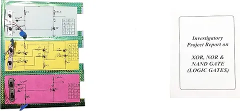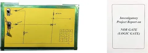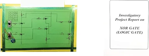
NAND GATE Educational Circuit Board
Code B07NYNGMGN
- Paid for and delivered by Amazon. The current price and the delivery date for your PIN code are shown there.
- Sold by Gurukul Technicals Institute, Delhi.
- Need a different topic, a custom version or a school order? Ask on WhatsApp.
In this project guide
Physics
About this model
This NAND gate educational circuit board demonstrates the NAND logic gate, which gives a 0 at its output only when every input is 1. It is a handy way to verify the NAND truth table and to understand why NAND is called a universal gate.
How it works
The science behind it
The idea the model demonstrates, in words you can use in your report and when you explain it.
The name NAND is short for NOT-AND, since the gate behaves like an AND gate with its output inverted. With inputs A and B, the output is Y = (A · B)′, read as 'A AND B, whole bar'. Its truth table: A = 0, B = 0 gives Y = 1; A = 0, B = 1 gives Y = 1; A = 1, B = 0 gives Y = 1; and A = 1, B = 1 gives Y = 0. So the output is 0 only when every input is 1. Its fame comes from being universal: NAND gates alone can build every other gate. Joining both inputs together gives a NOT gate, a NAND followed by a NOT gives AND, and inverting each input before a NAND gives OR, by De Morgan's theorem: (A′ · B′)′ = A + B. Chip designers can therefore build whole circuits, including memory, from one kind of gate.
Make it yourself
Make a NAND gate board and test it as a universal gate yourself
Build your own version from scratch, or use the steps to understand how the ready-made model is put together before you present it.
What you need 9
Step by step 9 steps
Fit the socket and wire the supply: pin 14 to positive and pin 7 to negative.
Wire each input switch to connect its input to positive when on, with its 10 kΩ resistor from the input to negative, so the input reads 0 when the switch is off and is never left floating.
Connect switch A to pin 1 and switch B to pin 2, with a green LED and 1 kΩ resistor from each input to negative so you can see which inputs are 1.
Connect the red output LED and its 1 kΩ resistor from pin 3 to negative.
Tie the inputs of the three unused gates (pins 5, 6, 8, 9, 12 and 13) to negative for now.
Fit the CD4011, switch on, set the four input combinations in turn, and record the output LED and the output voltage for each.
- Make a NOT gate
Free pins 5 and 6, join them both to switch A, and see pin 4 give the opposite of A.
- Make an AND gate
Feed pin 3 into both inputs of the second gate (pins 5 and 6) and move the red LED to pin 4.
- Make an OR gate
Invert A with gate 2 (pins 5 and 6 joined) and B with gate 3 (pins 8 and 9 joined), then feed pins 4 and 10 into gate 4 (pins 12 and 13). Its output, pin 11, is A OR B.
Read this first
Safety first
Go through these points before you build or switch anything on. Younger students should do this with an adult.
- CMOS chips can be damaged by static: touch a metal tap or other earthed metal before handling the CD4011, and hold it by its ends.
- Never leave a CMOS input unconnected; a floating input can make the chip draw extra current and warm up.
- Use only the 9 V battery, fit the IC with its notch matching the socket, and switch off before rewiring.
- Use the soldering iron only with an adult and rest it in its stand.
Troubleshooting
If something does not work
The usual problems with this model and how to fix them. Open a problem to see the fix.
The output LED flickers or changes when I touch the wires
An input is floating. Check that each input has its 10 kΩ pull-down resistor to negative and that unused inputs are tied down.
The output is always 1
The IC may not be powered, or the input switches are not reaching positive. Measure 9 V between pins 14 and 7, and check each input reads about 9 V when its switch is on.
The results look like an AND gate
The output LED is probably on the wrong pin, or the signal is passing through a second gate. Check that the LED is on pin 3 for the plain NAND test.
The IC gets warm
Switch off at once. The chip may be in the wrong way round, or an output is shorted to the supply. Check the notch and the wiring before trying again.
Exhibition day
How to present it
A running order for the exhibition table or the practical, step by step.
Go through all four input combinations and mark the truth table as you go.
Compare the NAND truth table with the AND truth table to show that each output is reversed.
Explain on a chart how NAND gates alone can make NOT, AND and OR gates.
Mention that NAND is one of only two universal gates, the other being NOR.
Practice
Viva questions
Practice questions on this model, with short answers. Try each one aloud before you open the answer.
Why is NAND called a universal gate?
Because any logic gate, and so any digital circuit, can be built using only NAND gates.
When is the output of a two-input NAND gate LOW?
Only when both inputs are HIGH (1).
How do you make an OR gate from NAND gates?
Invert each input with a NAND gate whose inputs are joined, then feed both into a third NAND gate; by De Morgan's theorem the result is A + B.
Name the other universal gate.
The NOR gate.
Project file
Project file outline
The headings of the project file, in order. Give each heading its own section and write it in your own words.
Free ebook: Writing a Science Project FileContents
- Aim: to verify the truth table of a NAND gate and show that it is a universal gate
- Introduction: digital signals, 0 and 1, and logic gates
- Theory: Y = (A · B)′ and the NAND truth table
- Pin diagram of the CD4011 and the circuit used
- Observations: output LED and voltage for each input combination
- NOT, AND and OR gates made only from NAND gates
- De Morgan's theorem checked from the readings
- Uses of NAND gates in computers and memory chips
- Conclusion and bibliography
Buying checklist
Before you buy
What to check before you order the model, and what to do when it arrives.
1Before you order
- Check with your teacher that logic gates are part of your current syllabus and which gates should be shown.
- Read the listing to see whether the board uses an IC or transistors, how the inputs are set and what powers it.
- Practise explaining why NAND is called a universal gate, as it is a favourite examiner question.
- Keep the box for transport.
- Check the delivery date for your PIN code on the marketplace, and order well before the exhibition or practical.
2When it arrives
- Run through the full truth table as soon as it arrives and note the results.
Next steps
Take it further
Ways to turn this model into a bigger investigation or a stronger exhibition entry.
Build an XOR gate from four NAND gates and verify its truth table.
Make a half adder from five NAND gates and show how computers add binary numbers.
Compare the CD4011 with a NAND gate built from transistors and discuss why chips are used instead.
Audience
Who it suits
Class 11 and 12 students working on digital electronics or Boolean logic in physics or computer science.
- SubjectPhysics
Free to read
Free ebooks for this topic
Free PDF ebooks from Gurukul Technicals Institute on the science, the making and the presenting of projects like this one.
- Free PDF ebook
Electricity and Magnetism Experiments
Hands-on experiments with cells, wires, bulbs and magnets
- Free PDF ebook
Physics Working Models Explained
Twenty classic models, how each works and how to make it
- Free PDF ebook
Your Science Exhibition Guide
Choose a project, build it, present it and answer the judges with confidence
- Free PDF ebook
Writing a Science Project File
How to write the report, from the cover page to the bibliography